SprintLayout - Reverse engineering a PCB
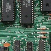
I did a similar video one year ago. This time I show a demonstration in real time (ish). Chapters: 0:00 - Intro 1:47 - Shout out. Some sun for Tommy Ovesen! 2:47 - Checking the scanned image 5:30 - Creating a component 7:59 - Wrong scale on vertical axis 8:53 - Measure, set DPI and scale the image in GIMP 15:35 - Using the scaled image 16:42 - All done. Ripping it up and doing it over! 18:20 - Placing parts (not needed) 18:51 - Placing VIAs 21:15 - Placing 2.54mm pitched VIAs using the grid 22:00 - Measuring and setting pad and hole size 25:07 - Copy, paste (CTRL C CTRL V), rotate, snap to grid. 35:13 - VIA placing time lapse 37:29 - Tracks 40:13 - Zones 41:43 - Automatic Ground Plane and Thermal Pads 43:00 - Lonely Islands, set distance to ground plane 44:25 - Photoview 44:43 - The Outline (Edge Cuts) 46:43 - Gerber and drill files 47:41 - Merry Christmas ! Tommy Ovesen's Channel: https://www.youtube.com/channel/UCJiYQTCfzbe5jZq2PXRaucg The Hackaday Article: https://hackaday.com/2019/12/31/reverse-engineer-pcbs-with-sprintlayout/ Other related videos: https://www.youtube.com/watch?v=g0nkLJ4YQ2c https://www.youtube.com/watch?v=2UtY5fDaRgo Music: Liptonman - Mitch / Dane - (1996) - C64 chiptune https://www.youtube.com/watch?v=lvlrbXknvsY
Download
0 formatsNo download links available.